When designing for an IC that uses the PCB as a heat sink, the datasheet usually only gives a single layout example – if that. But, what if you can’t implement your design exactly like the example? What are the relative effects of various compromises? It turns out that my intuition for which factors were most important was quite wrong.
I was reading an excellent application note from Texas Instruments, “AN-2020 Thermal Design By Insight, Not Hindsight” which lead me to do the detailed analysis I present here.
Summary (TL;DR)
The unexpected results:
- Putting solder mask over the surface copper foil REDUCES the thermal resistance of the PCB to still air. Don’t expose the copper!
- If the board is small, the series θ’s near the IC don’t matter much; but as the PCB gets larger, the θ’s near the IC will mostly determine the total θ of the layout.
- The thermal resistance of the FR4 is surprisingly low because it is thin.
- Copper planes without a direct metal connection to the IC can have a significant effect on the total thermal resistance.
- Both sides of the PCB radiate similar amounts of heat – even if one side has no copper at all.
Rules of Thumb:
These are in addition to the Rules of Thumb from the TI app note.
- Put solder mask over your heat sink area. Don’t expose the copper.
- Even with a single layer of copper, both sides of the PCB will radiate nearly equal amounts of heat.
- It is critical to get a direct metal connection from the heat source to the largest possible area of copper foil on any layer, internal or external.
- Unconnected planes can improve the total θ; but only if the directly connected copper area is greater than 5 cm² – 10 cm².
- A single layer of 2oz copper will yield a 25-35% improvement over 1 oz copper – but only if the copper area is greater than 50-60 cm². At 10 cm² the improvement is less than 10%.
- Copper areas larger 60 cm² yield diminishing returns.
- For a large PCB area, the total θ is primarily determined by the by the θ of the connection between the IC die and the copper foil and by the θ of the copper immediately surrounding the IC, so:
a. Avoid gaps in the copper near the IC! Get as much copper as you can, as close to the IC as possible. A 360° layout is best.
b. Connect the IC to as many planes as possible, as close to the IC as possible.
c. If possible, use thicker copper for the layer connected to the IC. - Layout for heat dissipation is complex; so design conservatively and test your layout as early as possible.
The Basics
There are many good explanations of heat ow calculation available; so, I won’t go into much detail on the basics. I include some of the basics here, only for context. Most IC data sheets list a maximum junction temperature. How do you know what the junction temperature is in your application? You can’t measure it directly. [Actually, some IC’s have an on board temperature sensor for this purpose – but, I digress…]
If you are familiar with Ohm’s law for electrical circuits there is a very useful analogy to be made with thermal calculations. In this analogy, you can think of heat flow (power dissipation) as an electrical current. Temperature is the same as voltage; heat flows from high temperature areas to lower temperature areas. And electrical resistance exactly corresponds to something called thermal resistance. Everything in the path of the heat flow presents some quantity of resistance to that flow. Thermal resistance is usually represented with the Greek letter theta (θ) and is given in the units “degrees C / Watt” (°C/W). This works just as it sounds, there will be θ degrees of temperature drop across the resistance for every watt dissipated through the resistance.
So, Ohm’s Law, “ΔV = I * R” becomes “ΔT = P * θ”, when applied to thermal resistance. Where ΔT is the difference in temperature across the thermal resistance, θ. And P is the power being dissipated. For DIP packages and SOICs, the IC datasheet may give a thermal resistance from junction to ambient, θja. Just as it sounds, this is the resistance to heat ow from the IC junction to the ambient environment (in still air/natural convection). You can think of this thermal resistance as the insulation value of the IC package. The temperature of the IC junction (Tj) is just the ambient temperature (Ta) plus the change in temperature due to the
power dissipation (ΔT).
ΔT = P * θja
Tj = Ta + ΔT
Tj = Ta + P * θja
Where the analogy between electrical resistance and thermal resistance becomes really useful is when heat sinks are used. The heat flow can be easily approximated by simple circuit-like analysis. If the IC is intended to be used with a heat sink its datasheet will include a value for the “junction to case” thermal resistance, θjc. And the heat sink data sheet should give a “case to ambient” thermal resistance, θca. This value will be a function of the rate of air ow across the heat sink. The combination of the IC case and the heat sink has a lower thermal resistance to ambient than the IC case alone. This new θja is just the sum of the IC’s θjc and the heat sink’s, θca.
θja = θjc + θca
Sometimes an electrically insulating pad will be placed between the IC and the heat sink. The pad’s datasheet may give its thermal conductivity (κ) instead of the thermal resistance (θ).
θpad = 1 / κ
The thermal resistance of the pad just adds in series with the other thermal resistances.
θja = θjc + θpad + θca
Some Insights Into SMD and PCB Heat Sinks
It is difficult to make a meaningful comparison between the relative effects of horizontal and vertical thermal resistances on a PCB. See the section at the end of this article for details on how I chose to do it.
For a very small board the θsa dominates the total θ. As the PCB gets bigger the total θsa gets smaller, so that θcu begins to dominate. At the size where θsa is smaller than θcu, the benefits of a larger PCB begin to vanish. Thicker copper or adjacent plane layers will decrease θcu and allow more PCB area to be effective. The thickness of the copper or number of plane layers is only important if the PCB area is large enough that θcu ≈ θsa. If the PCB is less than 10 cm², a single layer of 1 oz copper is nearly as good as thicker copper. Per the TI app note: At 60 cm², 2 oz copper can yield a 25% improvement over 1 oz copper. My calculations put it at about 28%.
It is interesting to note that the thermal resistance through the thickness of the FR-4 material is an order of magnitude less than that of the PCB to air. For 1 cm², 70 °C/W for 63 mils of FR4 vs. 1000 °C/W for the PCB to air. This means that even if you only have copper on one side of the PCB, the other side will dissipate almost as much heat into the air. And an interior layer with a direct metal connection will be almost as effective as a surface layer.
The front side is in parallel with the backside and also the FR4:
Total θ = 1/((1/(θ front side)) + (1/(θ back side + θFR4)) )
θFR4 vs θsa, for 1 cm²:
(λFR4) = 0.0023 W / (cm °C);
θFR4 = (1/0.0023) * (0.16 cm thick PCB) / 1 cm² = 70 °C/W
θsa (one side) = 1000 W/°C
θsa (two sides) = 1000 || (1000 + 70) = 517 °C/W
Effect of PCB Surface Finish
Covering the PCB heat sink copper with solder mask REDUCES θsa. From the On Semiconductor application note, “A Quick PCB Thermal Calculation for Power Electronic Devices with Exposed Pad Packages“:
“As noted above, for air velocities lower than 1 m/s, a significant fraction of this coefficient, as much as 35−40%, may actually be due to radiation, so surface emissivity may need to be considered. Shiny, metallic surfaces tend to have lower radiation contribution; matte−finish, non−metallic surfaces tend to have higher radiation contribution.”
From the Engineer’s Toolbox the emissivity coefficient of “copper, polished,” is between 0.023 and 0.052; while the emissivity coefficient of “black enamel paint” is 0.80 – I am using paint as an analog for solder mask. So paint/solder mask has an emissivity that is at least 15 times better than bare copper. Heat transfer by radiation is directly proportional to the emissivity coefficient of the material. Secondly, solder mask is so thin that it has virtually no thermal resistance. Therefore, I conclude that putting solder mask over the copper of a PCB heat sink is absolutely critical to maximizing thermal transfer from the PCB. A black matte mask is probably the best. I was very surprised by this conclusion.
Comparing the Lateral θcu to the Vertical θca
To compare the relative effect of horizontal and vertical thermal resistances I assumed a ring (annulus) cut out of an infinite unbroken plane of copper foil with an IC heat source at the center. The inner radius of this ring represents the radius of the IC’s thermal pad. An outer radius is calculated such that the ring has an area of 1 cm². In this way the horizontal and vertical thermal resistance can be compared for each added 1 cm². This ring section has a horizontal thermal resistance between the inside radius and the outside radius which can be compared with its thermal resistance to the ambient air.
area of annular ring = 1 cm²; Ro = outer radius; Ri = inner radius;
Ro = √((1/π) + Ri²)
For thermal resistance integrated across the annular ring:
θcu = ∫((1/λ) / (T * 2 * π * R)) dR
θcu = ((1/λ) / (T * 2 * π)) * ∫(1/R)) dR
θcu = definite integral from inner radius to outer radius
θcu = ((1/λ) / (T * 2 * π)) * (ln|Ro| – ln|Ri|)
for 1 oz copper: λ = 4 W/(°C·cm) ; thickness (T) = 0.0035 cm
θcu = 11.37 * (ln|Ro| – ln|Ri|)
The Graphs
This is the LibreOffice spreadsheet I used to calculate these graphs.
[link to spreadsheet]
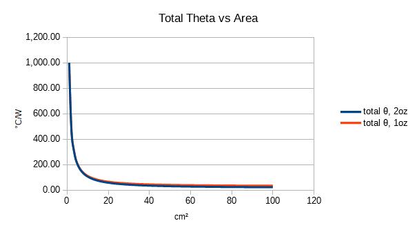
Total Thermal Resistance vs PCB Area
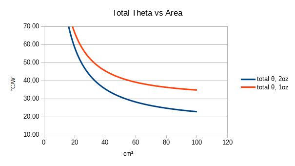
Total Thermal Resistance vs PCB Area (Detail)
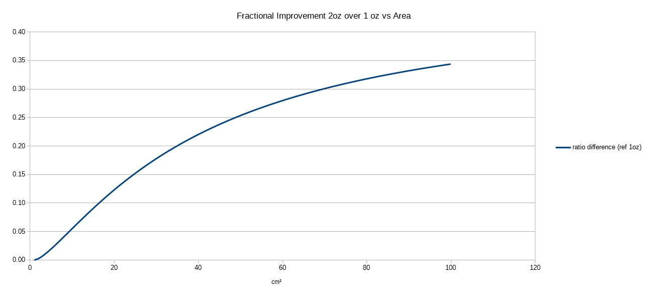
Relative Improvement of 2oz Over 1oz